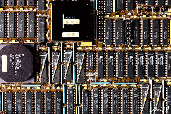
Sun Sparcstation 330 motherboard smart fix (1989)
<i>View <a href="http://commons.wikimedia.org/wiki/File:Sun_Sparcstation_330_motherboard_smart_fix.jpg" rel="nofollow"> in full resolution in Wikimedia</a> along with the <a href="https://commons.wikimedia.org/wiki/File:Sun_Sparcstation_330_Motherboard_(full_view).jpg" rel="nofollow">full motherboard</a> under CC public license. Part of the project to document the <a href="https://diis.unizar.es/" rel="nofollow">DIIS's</a> Computer Museum (EINA, Univ. Zaragoza)/ Ver la foto <a href="http://commons.wikimedia.org/wiki/File:Sun_Sparcstation_330_motherboard_smart_fix.jpg" rel="nofollow">en alta resolución</a> junto con <a href="https://commons.wikimedia.org/wiki/File:Sun_Sparcstation_330_Motherboard_(full_view).jpg" rel="nofollow">la placa completa</a> en Wikimedia bajo Licencia Creative Commons. Parte del proyecto de documentación del Museo de la Informática del <a href="https://diis.unizar.es/" rel="nofollow">DIIS</a> (EINA, Univ. Zaragoza)</i>
[Eng. /Esp.]
Sun Microsystems introduced its <b>Sun Sparcstation 330</b> with the SPARC architecture in 1989. SPARC was one of the first commercial materializations of a <i>reduced instructions set architecture</i> coming from the RISC project, led by <a href="https://en.wikipedia.org/wiki/David_Patterson_(computer_scientist)" rel="nofollow"> Prof. David Patterson</a> at the UC Berkeley, as MIPS was being led by <a href="https://en.wikipedia.org/wiki/John_L._Hennessy" rel="nofollow">Prof. John L. Henessy</a> at the Standford University. It was powered by a Cypress CY7C601 processor at 25 MHz along with a Texas Instruments 8847 FPU, and boasted a 72 MB RAM. My Department (<a href="https://diis.unizar.es/" rel="nofollow">Computing and Systems Engineering, DIIS</a> is its current name) bought one of these machines in 1990, which currently enjoys a well-deserved retirement in our Computer Museum, with its motherboard displayed inside a showcase. I pass next to it a dozen times a day, and recently realized that those <b>six crossed wires</b> with a yellow dot -likely a decoupling capacitor between GND and Vcc- can't be any other thing but <b>a late fix</b>. Someone didn't sleep /eat /... for quite a few days or weeks, who knows, until fixing <b>a (million dollars?) post-production bug</b>. I find this fix really beautiful, as it completely breaks up the dullness of the circuitry.
The two outstanding big chips are the first-level cache memory controller (left), and the (off-chip) L1 cache itself (above).
Sun Microsystems introdujo su <b>Sun Sparcstation 330</b> con arquitectura SPARC en 1989. SPARC fue una de las primeras materializaciones comerciales de una <i>arquitectura con repertorio reducido de instrucciones</i> proveniente del proyecto RISC liderado por el <a href="https://en.wikipedia.org/wiki/David_Patterson_(computer_scientist)" rel="nofollow"> Prof. David Patterson</a> en UC Berkeley, a la par que MIPS era liderado por el <a href="https://en.wikipedia.org/wiki/John_L._Hennessy" rel="nofollow">Prof. John L. Henessy</a> en la Universidad de Standford. Estaba alimentada por un procesador Cypress CY7C601 a 25 MHz junto con una FPU 8847 de Texas Instruments, y presumía de una memoria principal de 72 MB. Mi departamento (actualmente denominado <a href="https://diis.unizar.es/" rel="nofollow">Dept. de Informática a Ingeniería de Sistemas, DIIS</a>) adquirió una de estás máquinas en 1990, que actualmente goza de un merecido descanso en nuestro Museo de Informática, con su placa madre mostrada en una vitrina. Paso a su lado docenas de veces al día, y recientemente reparé en que esos <b>seis cables cruzados</b> con un punto amarillo encima –condensador de desacople entre GND y Vcc, con toda probabilidad- no pueden ser sino <b>un apaño tardío</b>. Alguien no durmió /comió /… durante bastantes días o semanas, quién sabe, hasta arreglar <b>un fallo (¿de millones de dólares?) aparecido en post-producción</b>. Este apaño me parece realmente bello, porque rompe completamente la aburrida regularidad del circuito.
Los dos grandes chips que sobresalen son el controlador de la memoria cache de primer nivel (a la izquierda), y la propia L1 (<i>off-chip</i>, más arriba).